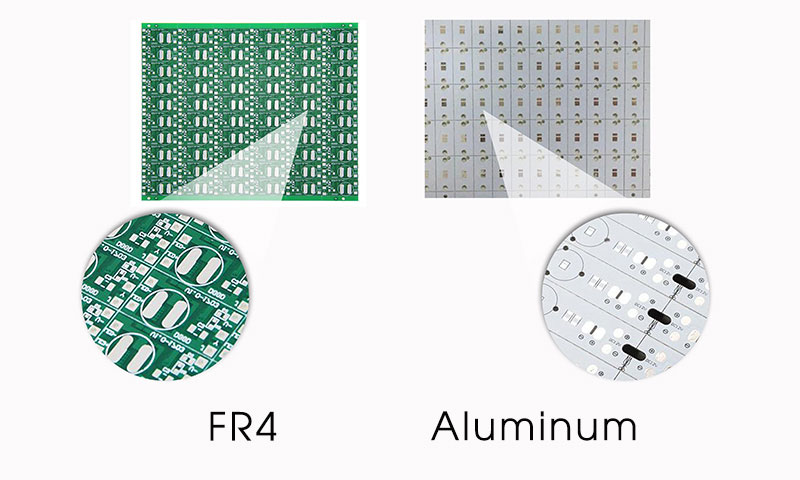
For the PCB boards now in application to LED headlight, there are mainly four kind of materials, Fiberglass(FR4) PCB, Aluminum PCB, Copper PCB and Ceramic PCB. It is a good deal to understand the distinctions for these four types PCB. Which PCB you choose depends on the circuit design construction of the headlight.
FR4 vs. Aluminum PCB
Price Comparison
In the cost comparison, the Aluminum PCB is more expensive than FR4, as well as more superior in performance.
Thermally Conductivity
Aluminum PCB has a great capability of thermal conductivity than FR4 which makes them play an important role in LED lighting technology.
Technology Practices
The thermal conductivity dielectric material of Aluminum PCB is a thermal bridge that connects the components and metal plate. It can transfer heat to the heat sink through the core automatically. An Aluminum backed PCB is assembled with aluminum backing, highly thermally conductive dielectric layer and the standard circuit layer. The circuit layer is a thin PCB bonding to the aluminum backing. As for FR4 PCB, it takes normal machining practices: drilling, routing, v-scoring, countersink counterbore. So it needs an additional heat sink to conduct heat in from the circuit layer. Or it will potential damaging hotspots.
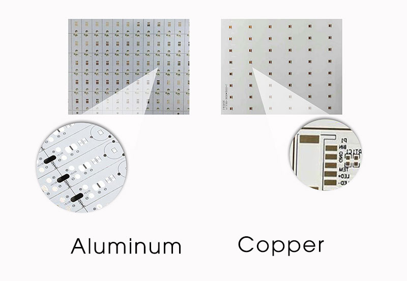
Aluminum PCB vs.Copper PCB
Price Comparison
The copper PCB is the most expensive types in metal core printed circuit board. The thermal conductivity is much better than aluminum PCB, this is usually used in high-frequency circuit design.
Thermally Conductivity
The thermal conductivity of copper PCB is double higher than that of aluminum PCB. The higher the thermal conductivity is, the higher the transfer efficiency is and the better the thermal diffusivity is. Copper PCB needs a thick copper foil for its large current carrying capability.
Technology Practices
As copper PCB is required to possess a great current carrying, a thick copper foil is needed, generally, the thickness is 35μm~280μm. A heavy copper PCB is produced in the same way by etching thick copper-clad laminated board material. It used plating technology and a combination of plating and etching to form the heavy copper features that result in trace sidewalls and ignorable undercutting. Copper PCB can be etched elaborate pattern and processed into a convex platform. The components can be attached to the platform to achieve the effect of excellent grounding and heat dissipation.
Ceramic PCB
Price Comparison
Ceramic PCB only can be seen in high-end products, the low-end products would not have. It is gradually taking place of the entire printed circuit boards to reduce the complexity of design and manufacturing as well we improve the performance.
Thermally conductivity
With the outstanding characteristic of high working temperature, low coefficient of expansion, high thermal conductivity, good insulation and thermally performance, makes a difference of the material itself, ceramics have more advantages over MCPCB. Ceramic PCB shows a high efficient thermally conductivity.
Technology practices
Ceramic PCBs are capable of providing optimal solutions for defeating thermal cycle failure because they share compatible CTE with the leadless ceramic chip carrier and feature higher thermal conductivity, higher stability and inertia. Three catalogs of ceramic PCB practices: high-temperature co-fired ceramic PCB, low-temperature co-fired ceramic PCB and thick film ceramic PCB.
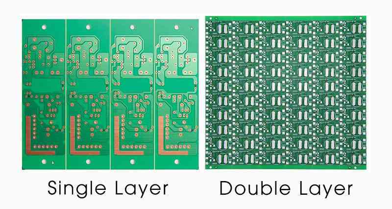
Single Layer PCB vs. Double Layer PCB
In generally, FR4, Aluminum PCB and Copper PCB all can be made into single layer PCB or double layer PCB.
Single Layer PCB
Single layer PCB is the most commonly used because it is easy to design and practice. This PCB covered a conducting material on the one side of the board. Single layer PCB with a good heat dissipation, each chip dissipates heat on one PCB, the LED headlight can be in a high lumen. But the width of two chip of two single layer PCB is too wide that is over 3mm. Limited by the width, it can not simulate the halogen bulb tungsten wire, the light beam is not clear with a dark area.
Double Layer PCB
This PCB covered two conducting material on both sides of the board. It provides a closer distance between the two sides of the chips, which is similar to the thickness of halogen bulb tungsten wire. For this result, it imitates the halogen bulb light-emitting forms, the light beam is better. However, both side of chips dissipate heat on one PCB, the heat cannot be too high, so it limits the lumen for LED headlight.
It does not rely on the area of PCB about the PCB heat dissipation problem. Thermal Management technology is another core part of PCB application. In the next article, I will discuss thermal management Printed Circuit Board (PCB) technology, especially SINKPAD Technology, it is the effective solution to automotive led lighting.